- 您现在的位置:买卖IC网 > Sheet目录2006 > LTC2704IGW-16#PBF (Linear Technology)IC DAC 16BIT QUAD VOUT 44-SSOP
LTC2704
5
2704fd
The
l denotes specications which apply over the full operating temperature
range, otherwise specications are at TA = 25°C.
Note 1: Stresses beyond those listed under Absolute Maximum Ratings
may cause permanent damage to the device. Exposure to any Absolute
Maximum Rating condition for extended periods may affect device
reliability and lifetime.
Note 2: The notation V+ is used to denote both V+1 and V+2 when the same
voltage is applied to both pins.
Note 3: Guaranteed by design, not subject to test.
Note 4: Measured in unipolar 0V to 5V mode.
Note 5: When using SRO, maximum SCK frequency fMAX is limited by SRO
propagation delay as follows:
fMAX =
1
2t9 + tS
()
, where ts is the setup time of the receiving device.
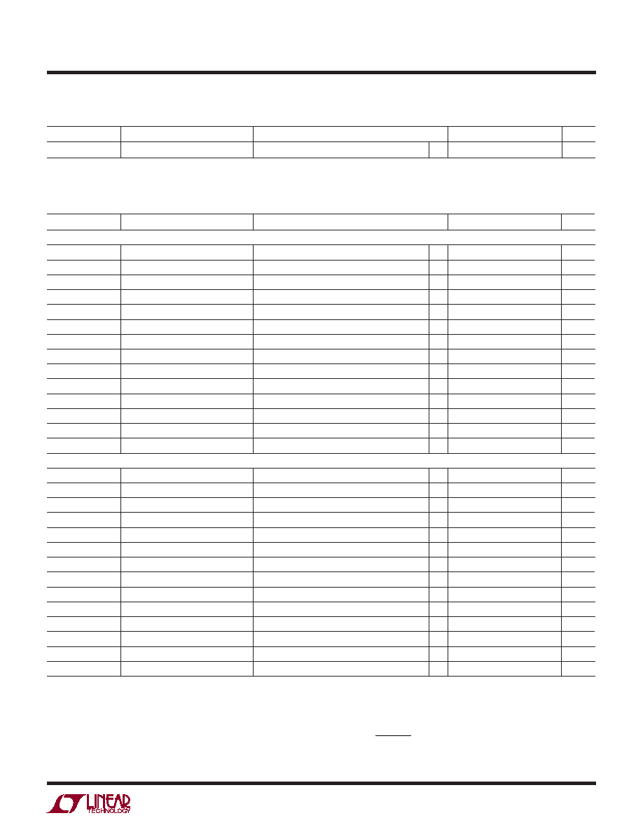
SYMBOL
PARAMETER
CONDITIONS
MIN
TYP
MAX
UNITS
CIN
Digital Input Capacitance
VIN = 0V (Note 3)
l
5pF
SYMBOL
PARAMETER
CONDITIONS
MIN
TYP
MAX
UNITS
VDD = 4.5V to 5.5V
t1
SDI Valid to SCK Setup
l
7ns
t2
SDI Valid to SCK Hold
l
7ns
t3
SCK High Time
l
11
ns
t4
SCK Low Time
l
11
ns
t5
CS/LD Pulse Width
l
9ns
t6
LSB SCK High to CS/LD High
l
0ns
t7
CS/LD Low to SCK Positive Edge
l
12
ns
t8
CS/LD High to SCK Positive Edge
l
12
ns
t9
SRO Propagation Delay
CLOAD = 10pF
l
18
ns
t10
CLR Pulse Width
l
50
ns
t11
LDAC Pulse Width
l
15
ns
t12
CLR Low to RFLAG Low
CLOAD = 10pF (Note 3)
l
50
ns
t13
CS/LD High to RFLAG High
CLOAD = 10pF (Note 3)
l
40
ns
SCK Frequency
50% Duty Cycle (Note 5)
l
40
MHz
VDD = 2.7V to 3.3V
t1
SDI Valid to SCK Setup
l
9ns
t2
SDI Valid to SCK Hold
l
9ns
t3
SCK High Time
l
15
ns
t4
SCK Low Time
l
15
ns
t5
CS/LD Pulse Width
l
12
ns
t6
LSB SCK High to CS/LD High
l
0ns
t7
CS/LD Low to SCK Positive Edge
l
12
ns
t8
CS/LD High to SCK Positive Edge
l
12
ns
t9
SRO Propagation Delay
CLOAD = 10pF
l
26
ns
t10
CLR Pulse Width
l
90
ns
t11
LDAC Pulse Width
l
20
ns
t12
CLR Low to RFLAG Low
CLOAD = 10pF
l
70
ns
t13
CS/LD High to RFLAG High
CLOAD = 10pF
l
60
ns
SCK Frequency
50% Duty Cycle (Note 5)
l
25
MHz
TIMING CHARACTERISTICS
ELECTRICAL CHARACTERISTICS The l denotes specications which apply over the full operating
temperature range, otherwise specications are TA = 25°C, V+1 = V+2 = 15V, V– = –15V, VDD = 5V, REF1 = REF2 = 5V, AGND = AGNDx =
REFG1 = REFG2 = GND = 0V.
发布紧急采购,3分钟左右您将得到回复。
相关PDF资料
LTC2751AIUHF-16#PBF
IC DAC 16BIT CUR OUT 38-QFN
LTC2752ACLX#PBF
IC DAC 16BIT DUAL CUR OUT 48LQFP
LTC2753AIUK-16#TRPBF
IC DAC 16BIT DUAL 48-QFN
LTC2754AIUKG-16#PBF
IC DAC 16BIT QUAD IOUT 52-QFN
LTC2755AIUP-16#PBF
IC DAC 16BIT CUR OUT 64-QFN
LTC2757ACLX#PBF
IC DAC 18BIT PAR 48LQFP
LTC2758AILX#PBF
IC DAC 18BIT SPI/SRL 48-LQFP
LTC2844IG#TRPBF
IC TXRX 3.3V MULTIPROTCOL 28SSOP
相关代理商/技术参数
LTC2704IGW-16#TRPBF
功能描述:IC DAC 16BIT QUAD VOUT 44-SSOP RoHS:是 类别:集成电路 (IC) >> 数据采集 - 数模转换器 系列:- 标准包装:2,400 系列:- 设置时间:- 位数:18 数据接口:串行 转换器数目:3 电压电源:模拟和数字 功率耗散(最大):- 工作温度:-40°C ~ 85°C 安装类型:表面贴装 封装/外壳:36-TFBGA 供应商设备封装:36-TFBGA 包装:带卷 (TR) 输出数目和类型:* 采样率(每秒):*
LTC2713CM-G
制造商:Lite-On Semiconductor Corporation 功能描述:
LTC-2721B
功能描述:LED 显示器和配件 Blue 3 Dig 0.28" Ht 466nm 3000ucd RoHS:否 制造商:Avago Technologies 显示器类型:7 Segment 数位数量:2 字符大小:7.8 mm x 14.22 mm 照明颜色:Red 波长:628 nm 共用管脚:Common Anode 工作电压:2.05 V 工作电流:20 mA 最大工作温度:+ 85 C 最小工作温度:- 35 C 封装:Tube
LTC-2721E
功能描述:LED 显示器和配件 3 Digit, Orange RoHS:否 制造商:Avago Technologies 显示器类型:7 Segment 数位数量:2 字符大小:7.8 mm x 14.22 mm 照明颜色:Red 波长:628 nm 共用管脚:Common Anode 工作电压:2.05 V 工作电流:20 mA 最大工作温度:+ 85 C 最小工作温度:- 35 C 封装:Tube
LTC2721G
制造商:Lite-On Semiconductor Corporation 功能描述:
LTC-2721G
功能描述:LED 显示器和配件 3 Digit, Green RoHS:否 制造商:Avago Technologies 显示器类型:7 Segment 数位数量:2 字符大小:7.8 mm x 14.22 mm 照明颜色:Red 波长:628 nm 共用管脚:Common Anode 工作电压:2.05 V 工作电流:20 mA 最大工作温度:+ 85 C 最小工作温度:- 35 C 封装:Tube
LTC-2721JD
功能描述:LED 显示器和配件 3 Digit, Red Low Current RoHS:否 制造商:Avago Technologies 显示器类型:7 Segment 数位数量:2 字符大小:7.8 mm x 14.22 mm 照明颜色:Red 波长:628 nm 共用管脚:Common Anode 工作电压:2.05 V 工作电流:20 mA 最大工作温度:+ 85 C 最小工作温度:- 35 C 封装:Tube
LTC-2721KF-06
制造商:Lite-On Semiconductor Corporation 功能描述:DISPLAY,CLOCK - Bulk